What is a CMOS : Working Principle & Its Applications
The term CMOS stands for “Complementary Metal Oxide Semiconductor”. This is one of the most popular technology in the computer chip design industry and it is broadly used today to form integrated circuits in numerous and varied applications. Today’s computer memories, CPUs, and cell phones make use of this technology due to several key advantages. This technology makes use of both P channel and N channel semiconductor devices. One of the most popular MOSFET technologies available today is the Complementary MOS or CMOS technology. This is the dominant semiconductor technology for microprocessors, microcontroller chips, memories like RAM, ROM, EEPROM and application-specific integrated circuits (ASICs).
Introduction to MOS Technology
In the IC design, the basic and most essential component is the transistor. So MOSFET is one kind of transistor used in many applications. The formation of this transistor can be done like a sandwich by including a semiconductor layer, generally a wafer, a slice from a single crystal of silicon; a layer of silicon dioxide & a metal layer. These layers allow the transistors to be formed within the semiconductor material. A good insulator like Sio2 has a thin layer with a hundred molecules thickness.
The transistors which we use polycrystalline silicon (poly) instead of metal for their gate sections. The Polysilicon gate of FET can be replaced almost using metal gates in large scale ICs. Sometimes, both polysilicon & metal FET’s are referred to as IGFET’s which means insulated gate FETs, because the Sio2 below the gate is an insulator.
CMOS (Complementary Metal Oxide Semiconductor)
The main advantage of CMOS over NMOS and BIPOLAR technology is the much smaller power dissipation. Unlike NMOS or BIPOLAR circuits, a Complementary MOS circuit has almost no static power dissipation. Power is only dissipated in case the circuit actually switches. This allows integrating more CMOS gates on an IC than in NMOS or bipolar technology, resulting in much better performance. Complementary Metal Oxide Semiconductor transistor consists of P-channel MOS (PMOS) and N-channel MOS (NMOS). Please refer to the link to know more about the fabrication process of CMOS transistor.
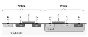
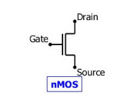
NMOS
NMOS is built on a p-type substrate with n-type source and drain diffused on it. In NMOS, the majority of carriers are electrons. When a high voltage is applied to the gate, the NMOS will conduct. Similarly, when a low voltage is applied to the gate, NMOS will not conduct. NMOS is considered to be faster than PMOS, since the carriers in NMOS, which are electrons, travel twice as fast as the holes.
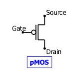
PMOS
P- channel MOSFET consists of P-type Source and Drain diffused on an N-type substrate. The majority of carriers are holes. When a high voltage is applied to the gate, the PMOS will not conduct. When a low voltage is applied to the gate, the PMOS will conduct. The PMOS devices are more immune to noise than NMOS devices.
CMOS Working Principle
In CMOS technology, both N-type and P-type transistors are used to design logic functions. The same signal which turns ON a transistor of one type is used to turn OFF a transistor of the other type. This characteristic allows the design of logic devices using only simple switches, without the need for a pull-up resistor.
In CMOS logic gates a collection of n-type MOSFETs is arranged in a pull-down network between the output and the low voltage power supply rail (Vss or quite often ground). Instead of the load resistor of NMOS logic gates, CMOS logic gates have a collection of p-type MOSFETs in a pull-up network between the output and the higher-voltage rail (often named Vdd).
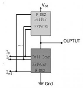
Thus, if both a p-type and n-type transistor have their gates connected to the same input, the p-type MOSFET will be ON when the n-type MOSFET is OFF, and vice-versa. The networks are arranged such that one is ON and the other OFF for any input pattern as shown in the figure below.
CMOS offers relatively high speed, low power dissipation, high noise margins in both states, and will operate over a wide range of source and input voltages (provided the source voltage is fixed). Furthermore, for a better understanding of the Complementary Metal Oxide Semiconductor working principle, we need to discuss in brief CMOS logic gates as explained below.
Which Devices use CMOS?
Technology like CMOS is used in different chips like microcontrollers, microprocessors, SRAM (static RAM) & other digital logic circuits. This technology is used in a wide range of analog circuits which includes data converters, image sensors & highly incorporated transceivers for several kinds of communication.
CMOS Inverter
The inverter circuit as shown in the figure below. It consists of PMOS and NMOS FET. The input A serves as the gate voltage for both transistors.
The NMOS transistor has input from Vss (ground) and the PMOS transistor has input from Vdd. The terminal Y is output. When a high voltage (~ Vdd) is given at input terminal (A) of the inverter, the PMOS becomes an open circuit, and NMOS switched OFF so the output will be pulled down to Vss.
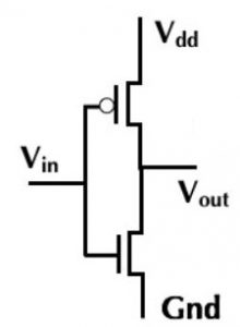
When a low-level voltage (<Vdd, ~0v) applied to the inverter, the NMOS switched OFF and PMOS switched ON. So the output becomes Vdd or the circuit is pulled up to Vdd.
| INPUT | LOGIC INPUT | OUTPUT | LOGIC OUTPUT |
| 0 v | 0 | Vdd | 1 |
| Vdd | 1 | 0 v | 0 |
CMOS NAND Gate
The below figure shows a 2-input Complementary MOS NAND gate. It consists of two series NMOS transistors between Y and Ground and two parallel PMOS transistors between Y and VDD.
If either input A or B is logic 0, at least one of the NMOS transistors will be OFF, breaking the path from Y to Ground. But at least one of the pMOS transistors will be ON, creating a path from Y to VDD.
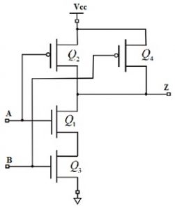
Hence, the output Y will be high. If both inputs are high, both of the nMOS transistors will be ON and both of the pMOS transistors will be OFF. Hence, the output will be logic low. The truth table of the NAND logic gate given in the below table.
| A | B | Pull-Down Network | Pull-up Network | OUTPUT Y |
| 0 | 0 | OFF | ON | 1 |
| 0 | 1 | OFF | ON | 1 |
| 1 | 0 | OFF | ON | 1 |
| 1 | 1 | ON | OFF | 0 |
CMOS NOR Gate
A 2-input NOR gate is shown in the figure below. The NMOS transistors are in parallel to pull the output low when either input is high. The PMOS transistors are in series to pull the output high when both inputs are low, as given in the below table. The output is never left floating.
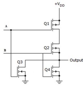
The truth table of the NOR logic gate given in the below table.
| A | B | Y |
| 0 | 0 | 1 |
| 0 | 1 | 0 |
| 1 | 0 | 0 |
| 1 | 1 | 0 |
CMOS Fabrication
The fabrication of CMOS transistors can be done on the wafer of silicon. The diameter of the wafer ranges from 20mm to 300mm. In this, the Lithography process is the same as the printing press. On every step, different materials can be deposited, etched otherwise patterned. This process is very simple to understand by viewing the wafer’s top as well as cross-section within a simplified assembling method. The fabrication of CMOS can be accomplished through using three technologies namely N-well pt P-well, Twin well, an SOI (Silicon on Insulator). Please refer to this link to know more about CMOS Fabrication.
A Lifetime of CMOS Battery
The typical life span of a CMOS battery is approximately 10 Years. But, this can change based on the utilization and surroundings wherever the PC resides.
Failure Symptoms of CMOS Battery
When the CMOS battery fails, then the computer cannot maintain the exact time & date on the computer once it is switched off. For instance, once the computer is ON, you may see the time and date like 12:00 PM & January 1, 1990. This fault specifies that the battery of CMOS is failed.
- The boot-up of the laptop is difficult
- The beep sound can be generated continuously from the motherboard of the computer
- The time & date have reset
- Peripherals of the computers don’t respond correctly
- The drivers of hardware have vanished
- The Internet cannot be connected.
CMOS Characteristics
The most important characteristics of CMOS are low static power utilization, huge noise immunity. When the single transistor from the pair of MOSFET transistor is switched OFF then the series combination uses significant power throughout switching among the two stated like ON & OFF.
As a result, these devices do not generate waste heat as compared with other types of logic circuits such as TTL or NMOS logic, which usually use some standing current even they don’t change their state.
These CMOS characteristics will allow for integrating logic functions with high density on an integrated circuit. Because of this, CMOS has become the most frequently used technology to be executed within VLSI chips.
The phrase MOS is a reference to the MOSFET’s physical structure which includes an electrode with a metal gate that is located on the top of an oxide insulator of semiconductor material.
A material like Aluminum is used only once however the material is now polysilicon. The designing of other metal gates can be done using a comeback through the arrival of high-κ dielectric materials within the process of the CMOS process.
CCD Vs CMOS
The image sensors like the charge-coupled device (CCD) & complementary metal-oxide-semiconductor (CMOS) are two different kinds of technologies. These are used to capture the image digitally. Every image sensor has its advantages, disadvantages & applications.
The main difference between CCD & CMOS is the way of capturing the frame. A charge-coupled device like CCD uses a global shutter whereas the CMOS uses a rolling shutter. These two image sensors change the charge from light to electrical & process it into electronic signals.
The manufacturing process used in CCDs is special to form the capacity to move charge across the IC without alteration. So, this manufacturing process can lead to extremely high-quality sensors about light sensitivity & fidelity.
In contrast, CMOS chips use fixed manufacturing procedures to design the chip and a similar process can also be used in making the microprocessors. Because of the differences in manufacturing, there are some clear dissimilarities among the sensors like CCD 7 CMOS.
CCD sensors will capture the images with less noise and huge quality whereas the CMOS sensors are usually more liable to noise.
Usually, CMOS uses less power whereas the CCD uses lots of power like more than 100 times to CMOS sensor.
The fabrication of CMOS chips can be done on any typical Si production line because they tend to be very cheap as compared with CCDs. CCD sensors are more mature because they are mass-produced for a long period.
Both the CMOS & CCD imagers depend on the effect of photoelectric to make the electrical signal from the light
Based on the above differences, CCDs are used in cameras to target high-quality images through lots of pixels & outstanding light sensitivity. Usually, CMOS sensors have less resolution, quality & sensitivity.
In some applications, CMOS sensors are recently improving to the point wherever they attain near equality with CCD devices. Generally, CMOS cameras are not expensive & they have a high life of the battery.
Latch-Up in CMOS
A latch-up can be defined as when the short circuit occurs between the two terminals like power and ground so that high current can be generated & IC can be damaged. In CMOS, latch-up is the occurrence of low impedance trail among the power rail & ground rail because of the communication between the two transistors like parasitic PNP & NPN transistors.
In the CMOS circuit, the two transistors like PNP & NPN is connected to two supply rails like VDD & GND. The protection of these transistors can be done through resistors.
In a latch-up transmission, the current will flow from VDD to GND straight through the two transistors so that a short circuit can occur, thus extreme current will flow from VDD to the ground terminal.
There are different methods for latch-up prevention
In latch-up prevention, high resistance can be placed in the trail to stop the flow of current throughout supply & to make β1 *β2 below 1 by using the following methods.
The structure of parasitic SCR will be beaked in the surrounding of transistors like PMOS & NMOS through an insulating oxide layer. The technology for latch-up protection will turn off the device once latch-up is noticed.
The testing services of latch-up can be done by many vendors in the market. This test can be done by a sequence of attempts to activate the structure of SCR in the CMOS IC whereas the related pins are checked when overcurrent flows through it.
It is advised to obtain the first samples from the experimental lot & send them to a testing lab of Latch-up. This lab will apply the utmost achievable power supply & then provide the current supply to the inputs & outputs of the chip whenever a Latch-up occurs through monitoring the current supply.
Advantages
The advantages of CMOS include the following.
The main benefits of CMOS over TTL are good noise margin as well as less power consumption. This is due to no straight conducting lane from VDD to GND, fall times based on the conditions of input, then the transmission of the digital signal will become easy & low cost through CMOS chips.
CMOS is used to explain the amount of memory on the motherboard of the computer that will store in the settings of BIOS. These settings mainly include the date, time, and settings of hardware
TTL is a digital logic circuit where bipolar transistors work on DC pulses. Several transistor logic gates are normally made-up of a single IC.
The outputs if CMOS drive actively in both ways
- It uses a single power supply like + VDD
- These gates are very simple
- Input impedance is high
- CMOS logic uses less power whenever it is held in a set state
- Power dissipation is negligible
- Fan out is high
- TTL compatibility
- Stability of temperature
- Noise immunity is good
- Compact
- Designing is very well
- Robust mechanically
- Logic swing is large (VDD)
Disadvantages
The disadvantages of CMOS include the following.
- The cost will be increased once the processing steps increases, however, it can be resolved.
- The packing density of CMOS is low as compared with NMOS.
- MOS chips should be secured from getting static charges by placing the leads shorted otherwise; the static charges obtained within leads will damage the chip. This problem can be solved by including protective circuits otherwise devices.
- Another drawback of the CMOS inverter is that it utilizes two transistors as opposed to one NMOS to build an inverter, which means that the CMOS uses more space over the chip as compared with the NMOS. These drawbacks are small due to the progress within the CMOS technology.
CMOS Applications
Complementary MOS processes were widely implemented and have fundamentally replaced NMOS and bipolar processes for nearly all digital logic applications. CMOS technology has been used for the following digital IC designs.
- Computer memories, CPUs
- Microprocessor designs
- Flash memory chip designing
- Used to design application-specific integrated circuits (ASICs)
Thus, the CMOS transistor is very famous because they use electrical power efficiently. They don’t use electrical supply whenever they are altering from one condition to another. Also, the complimentary semiconductors work mutually to stop the o/p voltage. The outcome is a low-power design that provides less heat, due to this reason, these transistors have changed other earlier designs like CCDs within camera sensors & utilized in most of the current processors. The memory of the CMOS within a computer is a kind of non-volatile RAM that store BIOS settings & the information of time and date.
I believe that you have got a better understanding of this concept. Furthermore, any queries regarding this concept or electronics projects, please give your valuable suggestions by commenting in the comment section below. Here is a question for you, why CMOS is preferable to NMOS?


Comments are closed.